Shipping by the hundreds of millions, MEMS devices are integral to our daily lives. Given the miniature size, low power and intelligent sensing capabilities of MEMS, it’s no surprise that microelectromechanical systems (MEMS) devices are found in every imaginable electronic product, from smartphones and cars to medical devices, environmental sensors and security systems. But there’s one pain point that has limited even greater growth of MEMS: Traditional MEMS manufacturing is inefficient, complex and costly.
Omnitron Sensors is changing the nature of MEMS manufacturing. Guided by a trio of industry experts, Omnitron is offering the first major manufacturing-level improvement to MEMS in over a decade. Omnitron calls it “a new topology for MEMS.”
Challenging established standards and assumptions around MEMS manufacturing processes, Omnitron’s new topology for MEMS simplifies system assembly and packaging, enhancing device performance and accelerating production for cost-sensitive, high-volume markets.
With such a new approach to MEMS manufacturing, how did Omnitron Sensors come to be?
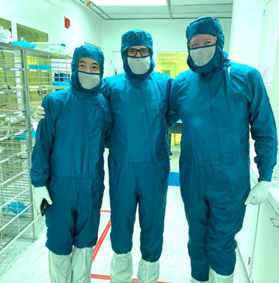
CEO & Co-founder Eric Aguilar, CTO & Co-founder Trent Huang and VP of Business Development Curtis Ray found one another in the field of advanced sensors. Eric and Trent met at Lumedyne Technologies, where they played leadership roles and helped to prepare the company for its acquisition by Google for $85M. Post-acquisition, they both stayed on with Google and ended up working on different projects — Eric as lead in avionics on Google’s Project Wing (later X, the moonshot factory) and Trent as lead technologist in quantum computing and in MEMS hardware. The two tech visionaries kept in touch as their careers progressed. And in February 2019, they co-founded Omnitron Sensors to realize the core IP that would change MEMS manufacturing as we know it.
Meanwhile, Curtis had been working in the industry since 1984, even before it was called MEMS. As both a thought leader in MEMS and a serial entrepreneur, Curtis found himself intrigued when an investor approached him to conduct due diligence on Omnitron Sensors. Impressed by Omnitron’s realization of a large step-scanning MEMS mirror that could be fabricated in volume by a commercial MEMS foundry— and fully aware of the transformative potential of the MEMS topology on which the mirror was based — Curtis joined the company to lead business development.
We interviewed Eric, Trent and Curtis about innovation in the MEMS industry and gathered their insights on Omnitron’s potential to transform MEMS manufacturing.
Question 1: Can you describe what Omnitron Sensors does at the 50,000-foot level?
Curtis: Omnitron is advancing the field of MEMS by combining bulk micromachining, surface micromachining, and SOI (Silicon on Insulator) techniques. Bulk micromachining involves creating grooves and other structures, often using DRIE (Deep Reactive Ion Etching). Surface micromachining uses layers of polysilicon and oxides to build thin, planar structures. While traditionally used for specific applications such as safety mechanisms in nuclear bombs, surface micromachining isn’t affected by electromagnetic pulses. At Omnitron we’re pioneering a hybrid approach that combines SOI and surface micromachining, creating a top layer that can move in and out of structures. This allows for versatile three-dimensional polysilicon structures for sensors and actuators.
Eric: As a result of this core IP for MEMS manufacturing processes, we’ve developed the first MEMS mirror that aligns to a LiDAR’s sub-micron-level tolerances without constant recalibration — and which is priced for cars instead of billion-dollar satellites. This has attracted the attention of Tier 1 automotive suppliers. With the capital in hand to manufacture our MEMS mirror and with Silex as our proven high-volume foundry partner, we’ve cleared the way to satisfy future demand from LiDAR suppliers.
That’s not to say we’re limiting ourselves to LiDAR. We’ve demonstrated broad applicability for our topology in diverse markets, including augmented reality, AI workflow, image stabilization, and laser spectrometry for toxic gas detection.
Question 2: What are the most exciting developments in MEMS that you’ve seen in the last decade?
Curtis: Until Omnitron, I haven’t seen much new for over 10 years. Omnitron’s actuator and capacitive sensors operate differently: instead of just using plates, we create deep trenches. The plates move in and out of the plane, increasing capacitance as they move farther out. Noise is a common issue in sensors, but our design minimizes stray capacitance. To meet our technical requirements, we flipped both the actuator and sensor. The mirror is actuated within a closed-loop system, consisting of a reflective silicon disk with actuators and sensors between the base and the mirror. The actuator moves the mirror, and the sensor precisely measures the movement. This same sensor and actuator setup can also be applied to microfluidics.
Trent: The implementation of the piezoelectric (PZT) process is a significant advancement because it opens new ways to activate devices and systems. Yet it’s only been in the past decade that PZT has been qualified as a MEMS technique. The main challenge now lies in qualifying PZT for the rigors of automotive.
Question 3: What are your hopes for the Omnitron Sensors?
Trent: I hope our technology revitalizes the MEMS industry and enhances R&D in education as well. The potential of sensor integration in our world is still largely untapped, far beyond what we currently see. As AI becomes more prevalent, it’s clear that we need reliable hardware to integrate sensors into our daily lives. The Internet of Things (IoT) has been a promising concept, but producing affordable and reliable sensors has been challenging. Small sensors often drift, but our technology aims to solve these problems and make widespread sensor use a reality.
Eric: At Omnitron Sensors, we aim to revolutionize robotics by advancing sensors that enable real-world operation. By disrupting the MEMS market with our new topology, we are not only driving innovation but also fostering an environment where major steps can be taken in chip technology. Our goal is to unlock future innovations in fields that are beyond current imagination
Meet our Leadership Team
Eric Aguilar, co-founder and CEO, is an award-winning entrepreneur and visionary leader in the field of advanced sensor systems for complex systems such as robotics and autonomous platforms. His expertise includes leading teams at renowned companies such as Tesla, where he managed a crew of 300 engineers on the firmware for Model 3, and at X (the moonshot factory), where he spearheaded the development of Google Project Wing, an autonomous drone delivery service.
Eric’s leadership roles at Argo AI and at Lumedyne Technologies (acquired by Google) underscore his impact on the industry. Earlier in his career, Eric did pioneering work in building sensors for drones at US Navy Research Labs.
With a BS in Electrical Engineering from California State Polytechnic University and advanced studies at the University of Southern California, Eric continues to shape the future of sensor technology.
Dr. Trent Huang, co-founder and CTO, brings extensive experience in optical, microwave, micro-/nano-fluidic, and biological MEMS sensors, actuators, and microfabrication to Omnitron Sensors, where he leads the company’s technology teams to drive organizational growth.
Trent holds numerous patents, and his expertise in theories, applications and productization of micro-/nano-systems has consistently delivered transformative solutions that allow Omnitron to break through the barriers of MEMS manufacturing. With a strong track record of leveraging emerging technologies to solve complex business challenges, he thrives in dynamic environments where creativity and agility are paramount.
Prior to Omnitron, Trent led teams of scientists and engineers at Google in the areas of quantum computing, and in MEMS hardware and system technologies for Android products. Trent has held leadership positions in MEMS engineering at Lumedyne Technologies (which Google acquired during his tenure) and at Tessera Technologies. His professional experience also spans bio-compatible MEMS, molecular nanotechnology, and optical technologies.
Trent earned a BS in Physics at the University of Science & Technology of China, an MA in Physics at the University of Virginia, and a PhD in Electrical Engineering from Cornell University.
Curtis Ray, head of business development, cultivates relationships with employees, customers and advisors who are driven to change the world through life-enhancing technology.
Considered one of the early thought leaders in MEMS technology, Curtis’s expansive career includes developing and selling a MEMS foundry, and launching MEMS sensors, micro-opto-electromechanical (MOEMS) mirrors, and multiwavelength optical transceivers to commercial markets.
With 31 patents, and four companies built and sold under his belt, Curtis possesses that unique combination of technical excellence and business acumen that are vital to a startup’s success. Curtis has dedicated a significant part of his career to guiding aspiring engineers and entrepreneurs, evident in his long-term involvement with First Robotics.
Curtis earned a BSME from Purdue University and an MBA from Haas School of Business at University of California, Berkeley.
Together, Eric, Trent and Curtis are at the forefront of sensor innovation, each bringing unique expertise and vision to Omnitron Sensors. Their collective efforts are unlocking the full potential of MEMS to add intelligence to the electronic products in our lives.