A New Paradigm for MEMS Manufacturing
Billions of electronic products rely on MEMS devices. Our cars and smartphones. Every wearable you can imagine. Our security systems, our environmental sensors, and our health and medical devices. From the smart home and the smart farm to the smart city, MEMS devices are ubiquitous.
But complex, expensive and laborious ways of manufacturing MEMS devices have slowed the growth of a microscale technology that’s critically important to the functionality of the electronics we have today and those we’ll have tomorrow.
We’re passionate about MEMS technology. That’s why we rebuilt the manufacturing process for MEMS from the ground up.
Our core IP
We took the first step, looking at existing silicon processes to see how we could address pain points, using tools that are available on every MEMS manufacturing floor. Through clever rearrangement of existing modules that now leverage our new topology for MEMS, we’ve simplified how systems are assembled. Our process IP streamlines the assembly process and improves device performance, speeding the production of leading-edge MEMS sensing technology for price-sensitive, high-volume markets.
How we do it
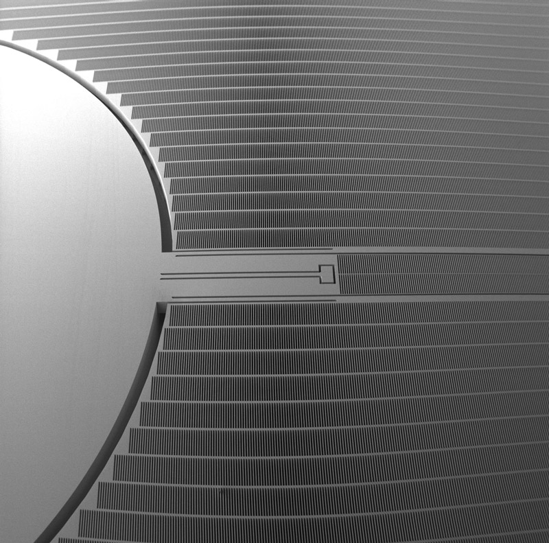
We use silicon on insulator (SOI) and surface machining to create a hybrid design that can have three dimensions of polysilicon for the MEMS sensor and the actuator. It’s like a microelectromechanical origami.
We achieve higher capacitance per unit area by extending packaging into the third dimension. This allows for more flexible system alignment, which is critical for optical applications and which lets us achieve a more complex package.
Higher capacitance per unit area also reduces cost. Think of this: If a wafer costs up to US$5,000 per wafer, and you can get 1,000 chips from it instead of just 100, you’ve achieved an order of magnitude in cost savings. That’s a big difference to your bottom line.